
Get Quote


YANGZHOU POSITIONING TECH CO., LTD.
News
- Full-digital IGBT IF induction power supplyFull digital IGBT induction power supply (series type) function introduction: This power supply is a true full-digital power supply. With constant current, constant power, constant temperature, and other ways of power regulation. There are internal control, external control, screen control and other control methods. Powerful management function and setting function, monitoring function, diagnosis, protection function, with powerful communication function. The performance is stable and reliable, and the melting rate reaches 460KW / H-530KW / H per ton, while the melting rate of domestic and foreign peers per ton is basically 600KW / H-700KW / H, and the energy saving effect is far ahead. The energy-saving induction IF power supply working frequency 50 HZ-30000 HZ, the power 50KW-20000KW, is applied to the smelting of non-ferrous and ferrous metals; in metallurgy, casting, diathermy, heating, vacuum smelting and other fields.
2024 03/11
- Operators who keep their word and promiseYangzhou Positioning Tech Co., Ltd. Operators who keep their word and promise No abnormal operation No breach of promise No major negative comments Issued by: Member unit of Shanghai Credit Services Industry Association
2023 11/07
- Use of the IGBT module for parallel design considerationsUse of the IGBT module for parallel design considerations Due to the high production cost, the price of 1200V I GB T module greater than 400A in the market. As for the standard 1200V, 200-400A 62mm module, due to the relatively stable technology and product, good product versatility and easy to replace, it is the most economical way to use multiple standard IGBT modules in parallel to improve the current rating at this stage.However, due to the inconsistency of IGBT own parameters and the possible asymmetry caused by circuit layout, it is not a simple job to use IGBT module for parallel design. Unreasonable selection of components as parallel or components can easily fail the device and damage the lines on the main system.Therefore, this paper, from the successful experience of the application department in the client and the test equipment in the factory, and proposes the importance of using star IGBT module for parallel design. Modules generally larger than 100A themselves are made of several chips in parallel, although manufacturers can use chips on the same wafer to connect in parallel to reduce the parameter difference of the module itself.However, it still needs to take into account the individual differences between the resulting module parameters.At the same time, the symmetry of the circuit is a very important influence on parallel, which can be expounded from the two aspects of static and dynamic, from the difference of parameters and the difference of circuit symmetry. Factors affecting the parallel and static mean flow of modules In actual use, the working state of IGBT module is mainly in the conduction and switch transient, and the conduction stage is relatively long and the current is large. This section has a great impact. Start from the static conduction state. 1.1. The main reasons for affecting the parallel average flow of the module are the following 4 points A) Effect of saturated pressure drop Vce (sat) The b) Effect of the impedance asymmetry of the parallel power circuit The c) Effect of the gate pole drive voltage Vge The d) Effect of the on voltage V th e) Effect of diode conduction pressure drop Vf 1) Problems with different Vce (sat) in parallel: In many cases, the average person thinks that the Vce (sat) generated by the current flowing through the IGBT is a fixed value, which is a misconception. Vce (sat) actually refers to the pressure drop generated by the rated current.For IGBT, the conduction pressure drop is a function of the current at the same V ge. For the two IGBT connected in parallel, the pressure drop generated by the positive guide pass when opening the steady state is equal.Thus, the equilibrium of the current distribution depends on the differences in the output characteristics of the various IGBT s in parallel. Figure 1 shows the difference in the current distribution of two different output characteristic IGBT s in parallel (the same Vce of two IGBT in parallel). Figure 1 The IGBT situation after the average flow in parallel with different output characteristics Figure 2 Schematic diagram of the average flow when connected in parallel The V shown in Figure 1T1And VT2For two identical IGBT models in parallel, Figure 2 shows that the output characteristics of the two IGBT's are slightly different.iC1And iC2respectively VT1And VT2In having the same tube pressure drop (UCE1=UCE2) The collector current below, I indicates the rated current of this type of IGBT, Vcesat1And Vcesat2Represents ote the saturated pressure drop of two I GBT at rated current.It can be approximate that: R1=(Vce sa t 1-Vo1)/I (1) R2=(Vce sa t 2-Vo2)/I (2) UCE1=Vo1+R1×iC1(3) UCE2=Vo2+R2×iC2(4) When connected in parallel, the UCE1=UCE2=Uce,Is iC1=( Uce-Vo1 )/R1=( Uce-Vo1 )×I/(Vcesat1-Vo1) iC2=(Uce-Vo2)/R1=(Uce-Vo2) ×I/(Vcesat2-Vo2) Since these two IGBT's are of the same type, Vo1 Vo2 =Vo then Therefore, if the current of two parallel I GBT modules is I, the current of two IGBT module with different Vce can be calculated as follows: iC 1=( Uce-V o1 )/R 1=( Uce-V o1 )×I/(Vcesa t 1-V o1)=(Uce-V o )×I/(Vcesa t 1-V o ) iC 2=(Uc e-V o2)/R 1=(Uc e-V o2)×I/(Vc e s a t 2-V o2)=(Uc e-V o )×I/(Vc e s a t 2-V o ) Take the most common GD200HFL120C2S, for example: Suppose a larger value of Vcesat1 2.5V (125℃), smaller value Vcesat2For 2.1V, (125℃), Vo =0.8V Assuming a larger value of Vcesat1Is 2.2V, with the smaller value of Vcesat1For 2.1V, be checked by the data manual The typical Vo to is =0.8V If the Vcesat difference is 0.1V, even if the output current required by the parallel module is io =200A, the current difference of the lower IGBT module of another Vce (sat) is 6A.In practice, there will be more loss than another IGBT module, although the IGBT chip is in a large current It has a positive temperature coefficient, so when the two I GB T modules are in parallel, it is recommended that the difference between V ce (sa t) should not exceed 0.2V. If unavoidable, it is recommended to leave a large margin on the steady state temperature to compensate. 2) Uneven shunt caused by the impedance asymmetry of the power circuit Fig. 2 Effect of impedance of main circuit circuit It is generally believed that the difference in the parallel line storage of the bus will result in the circuit impedance. Therefore, if the IGBT module using V c e (s a t) difference is less than 0.2V, the symmetry of the bus line must be taken into account. In fact, the impact of this part is actually low, such as the equivalent circuit diagram 2, the RE1And RE2Equivalent to the serial connection of two resistors and the original two uniform flow average branch, if the impedance is inconsistent, it will cause the uniform flow is inconsistent, such as RE1> RE2, That Yao RE2There will inevitably be more current above the branch, causing uneven imbalance and vice versa.Take GD200HFL120C2S as an example: The actual current required for the parallel module is i o =200A, each module is actually 100A, and the pressure drop on the actual module is Uce =1.7V Suppose the bronze medal cross-section is 410-5m2, The master row length of module 1 is 0.8m, the master row length of module 1 is 0.6m, and the thermal resistance rate at 30℃ is 1.810-8Ω *m Compared to the influence of V c e (s a t), the influence of power loop asymmetry is relatively unnecessary when static apprehensive.However, the bus will also introduce the lead inductance, which will have a great impact on the dynamic average flow, which will be further discussed in the future. 3) Influence of the gate pole drive voltage Vge current ICThe module flowing through the IGBT driven by the gate voltage Vge generates the conduction pressure drop Vce, which is not only related to the flowing current Ic, the V ce (sat) provided above, but also directly related to the gate drive voltage Vge. Conversely, at different drive voltage Vge, with the same Vce in parallel, the current Ic through the two is naturally different. Figure 3. Output characteristic curve of the IGBT module From Figure 3, we can clearly see that, As in Vge =13V, at Vce =2.5V, through the current Ic 255A As in Vge =15V, at Vce =2.5V, through the current Ic 285A Therefore, the drive circuit design needs to pay very much attention, and be sure to ensure the drive voltage of the parallel module. It should be emphasized here that the gate voltage Vge discussed above refers to the two ends of the IGBT gate, not the output voltage of the drive plate, and careless customers often make this mistake.As can be seen from Figure 4, there is a gate resistance between the drive chip and the gate pole, and the electrical connection from the drive chip to the I GBT gate pole, which is the gate lead of the machine usually seen on the machine, and the parameter difference of the drive component and the gate lead will be compared with the moment of opening and closing Highlight, will cause the added to the IGBT gate voltage and the output voltage inconsistency.This will not be a problem in the steady state because the gate belongs to a high resistance state. Figure 4 Schematic diagram of the module driver 4) Effect of the open voltage, Vth Because the voltage applied by the voltage of the drive circuit to the gate is a process from the negative pressure to the applied positive voltage (if there is a negative pressure off), the current I cannot flow through the module before the gate voltage Vth, so the IGBT of the smaller Vge (th) will open earlier and turn off later.Since this effect is mainly at the moment of opening, and it can be known from the transfer characteristic curve of FIG. 4, the I c current is very small when the drive voltage is V t h. Generally, the difference of module Vth of the same type is within 0.5V, so the effect of opening voltage Vth is relatively weak. 5 Transfer characteristics of the I GB T module 5) Effect of the diode Vf In the inverter and other applications, the IGB T module reverse parallel diode needs to bear a lot current.The effect of Vf of the diode on the mean flow is exactly the same as that of Vce (sat) on the mean flow, only the I GB T affected by V ce (sat) and the V f of the diode. R1=(V f-Vo1)/I R2=(V f-Vo2)/I Uf1=Vo1+R1×if1Uf2=Vo2+R2×if2 (1) (2) (3) (4) When Uf1=Uf2=Uf is connected in parallel, then iC1=( Uf-Vo1 )/R1=( Uf-Vo1 )×I/(Vf1-Vo1) iC2=( Uf-Vo2)/R1=( Uf-Vo2) ×I/(Vf2-Vo2) Since these two diodes are of the same type, Vo1 Vo2 =Vo Therefore, if the current of two parallel IGBT modules is I, the current of two IGBT module with different Vce can be calculated as follows: iC1=( Uf-Vo1 )/R1=( Uf-Vo1 )×I/(Vf1-Vo1)=( Uf-Vo ) ×I/(Vf1-Vo) iC12=(Uf-Vo2) / R2= (Uf-Vo2) I / (Vf2-Vo2) = (Uf-Vo) I / (Vf2-Vo) Common 150A module is column, Assuming that the larger value V f is 2.2V and the smaller value Vf is 2.1V, the typical Vo found by the data manual is =1.3V Factors affecting parallel dynamic flow The main reasons affecting the parallel dynamic mean flow of modules are the following 3 points A) Dynamic parameters of the IGBT itself The b) parasitic induction of the drive circuit c) The parasitic inductance of the power circuit 1) Uneven distribution caused by I GB T's own parameters The main factor affecting the current equilibrium at the switching time is the transfer characteristics of the parallel device. Figure 3. Comparison of the transfer characteristics of the parallel modules Comparison diagram of two parallel module properties with inconsistent transfer characteristics shown in Figure 3.In FIG. 3, when the same drive voltage V is applied to the parallel moduleGEWhen, the steep IGBT module will withstand more current, and the switching loss will also become larger.2) Parasitism of the drive circuit and uneven shunt caused by the inductance Combined with the gate-level parasitic capacitance of the IGBT, the parasitic inductance of the driving circuit may cause severe oscillations, causing fluctuations in the gate voltage.The parasitic inductance of the emitter can cause the switching degree variation. IGBT gate pole drive circuit RG, lead inductance LGLE,, and IGBT input capacitance CinThe process of opening and switching is a typical R L C series circuit response.In Figure 4, the resistor R corresponds to RG, L, corresponding to the inductor LG+LE, Capacitor C corresponds to the input capacitor Cin. For the on and off process, just uC(0) And the USThe difference of the value of the 1920s, when turned on, uC(0)=-10V ,US=15V (the general drive voltage is often + 15V on, -10V off), and when off, uC(0)=15V ,US=-10V Due to the parasitic lead inductance of LGLEThe existence, will increase the possibility of gate pole shock, need to avoid the generation of this lead inductance.In the actual line, the length of the gate lead and the area of the gate lead loop (such as a twisted pair) can be reduced.While the gate electrode resistance, RGIt needs to be added separately to start up with better results. Figure 4 Transmitter-parasitic inductance of the drive circuit 3) Uneven distribution caused by the parasitic inductance of the power circuit The parasitic inductor of the power circuit mainly consists of two main parts, namely, the collector parasitic inductor Lc And the emitter-parasitic inductor Le, as shown in Figure 5. When the gate voltage drive waveform is switched, the power loop is being rapidly changing, and the speed is at a subtle level. The inductors L c and L e of the power loop will play a role in hindering the change of current, resulting in the slow conversion speed.In parallel, due to the relationship between layout and wiring, there are great differences in the parasitic inductance of the power circuit, which is bound to cause dynamic diversion imbalance.Here especially emphasize the collector parasitic inductor L c, due to the parallel current is very large, the current is off, because the off speed, current is very large, collector parasitic inductor Lc tend to produce large and bus voltage direction reverse momentum, and bus voltage superposition on IGBT above IGBT, impact, if more than IG BT rated voltage, is bound to cause damage to IGBT. Figure 5. Parasitic inductance of the power circuit Therefore, designers need to optimize the circuit design of the main circuit according to the actual conditions. For example, if the copper row can be used, not copper wire, if the cost allows, adopt the main loop mode. 1) Selection of modules From the static flow, N PT IGBT module has positive temperature coefficient is suitable for parallel.On the other hand, parallel modules, especially those on the same bridge arm, can use the same batch of modules as far as possible, so as to ensure the consistency of parameters to the maximum extent. 2) Drive loop design When the IGBT module is in parallel, influenced by the inductance of the gate circuit wiring and the input capacitor of IGBT, the gate voltage sometimes rises. In order to prevent this oscillation, the gate resistance should be connected on the IGBT gate. When the emitter wiring of the driving circuit is connected at a different position from the main circuit, the transient current distribution of the parallel-connected IGBT becomes unbalanced.The IGBT module has the auxiliary emission extremes used by the drive circuit, be sure to use this terminal, The driving wiring can be equal, and the transient current imbalance caused by the wiring method of the driving circuit can be suppressed. Door-pole wiring is also critical: A) The drive line should be short, and the effect of the twisted pair line will be better; b) The drive line should be far away from the main circuit, try to achieve orthogonal layout; c) Each drive line moves separately and is not tied together. 3) Line layout When the resistance part and the inductance part of the main circuit wiring are unequal, the current distribution of the parallel connected elements will produce uneven uniform flow.In addition, if the inductance parasitic by the main circuit is large, the surge voltage will increase when IGBT is turned off. Therefore, in order to reduce the inductance of the circuit, the parallel connected IGBT module should be configured as closely as possible, and the wiring should maintain good symmetry. In order to reduce the line sense and line resistance, the DC bus to avoid using cable wire, this wire self-sensing and mutual sense are very poor, and the thermal conductivity is very poor.Copper strip can effectively solve the self-perception and heat dissipation, but the mutual feeling is still very large.Laminated bus is multi-layer copper plate stacked together, layer and layer directly using insulation heat conductivity isolation, effectively solve the self-sensing, mutual sense, heat dissipation, but also has the role of impedance and reduce E M I, is a relatively ideal bus form, as shown in the figure below: Figure 6 layer stacked bus diagram In addition, the modules should be mounted on the same radiator close to each other to obtain optimal thermal coupling with uniform temperature and minimize the effects of Tj and Vth. conclusion: This paper analyzes the factors affecting the average flow of parallel modules, combined with Star's equipment, in addition to providing products more suitable for parallel, but also proposes the attention of using IGBT modules for parallel design from the perspective of application, so that designers can have a deeper understanding of IGBT parallel and can follow the design. reference documentation: 1.I n t e r n a ti on a l R ec tifi e r A pp li ca ti on N o t e s .AN 990. A pp li ca ti on C ha r ac t e ri za ti on o f I GB T s [ Z ] ,2002. 2.D yn e x S e m i c ondu c t o r .AN 5505. P a r a ll e l O p e r a ti on o f D yn e x IGBT M odu l e s[Z ] ,2001. 3 Sun Qiang, Wang Xueru, Cao Yuelong, high-power IGBT module parallel average flow problem research [J] Power electronics technology in 2004 4. Tong Shi Bai Hua Chengying simulation electronic technology foundation [M].Higher Education Press, 2001
2022 05/20
- Short circuit of IGBT in the system and its protection,IGBTmoduleIGBTmodule Method protects the upper and lower pipe through. The photocoupled protection IGBT is achieved by detecting the C-E voltage, and according to the relationship between V ce and Ic, when Ic rises rapidly, Vce follows up.When the Vce value rises to the protection point voltage, the optical coupling will turn off itself and send the error signal to the DSP, the whole process is generally between 5 and 10us.Because such protection is very highly sensitive and has poor accuracy, it is only suitable for short-circuit protection.Figure 2 shows the diagram of Vce and Ic of GD200HFL120C2S. With the rise of Vce, the increase of IC is increasing. The Ic at + 7V actually far exceeds the short-circuit current of the module.When doing dynamic short circuit test, L, Vg, tr, tf and other parameters have strict and stable control, and the current is generally controlled at 8-10 times Ic, as shown in Figure 3. However, the short circuit is tested on the system, and the current will often rise higher due to the switch characteristics, the circuit load and the interference. Common short-circuit protection to drive optical coupling (I) PC929 PC929 is a common drive optical coupling in the inverter industry, with short circuit protection function (PC923 without protection). Because its output peak current is only 0.4A, driving high power IGBT needs to be amplified at the rear end to drive IGBT.How much current of the module that the P C 929 can drive depends on the choice of the tube. As long as the PC929 can push the tube and the tube can push the IGBT, then it can be achieved. Figure 3 shows the PC929 internal protection circuit: 1, When the IGBT is turned off, the 9-foot C voltage is pulled to zero. 2. When IGBT is turned on, Vcc charges the Cp through Rc, with the charging voltage exceeding + 7V, and O2 transmission With the soft turn-off, FS sends the error signal CPU at the same time, FS is effective at the low level, and the charging speed of Cp is determined by Rc and Cp. 3. When IGBT is turned off, C is quickly pulled down, and the down speed is much greater than IGBT off speed. Many people reflect that P C 929 is prone to misaction, but the mechanism of misaction is not very clear. Some people think that the protection time is too short, while others think that THE pressure drop of IGBT is too large.Then let's discuss the reason why P C 929 misacts, which is very important for the protection circuit design of IGBT. In theory, the larger the Vce (sat), the faster the IGBT reaches the protection voltage + 7V in the linear zone, which is correct, but is not the cause of misaction.The value of Ic corresponding to the saturation pressure drop of + 7V is far greater than the saturation pressure drop of the maximum overload current, while the pressure drop of the general chip is only below 1V, and this gap will not cause misaction in the non-short circuit state. When IGBT is opened normally, the main reason for misprotection error is the time of V c e falls when IGBT opens, and the charging time of C p. See Figure 4. The power supply Vcc charges the Cp through the Rc, with the charging voltage of Ucp. If Vce goes down along a path, then Vce has dropped below + 7V before Ucp reaches + 7V, then the 9-foot voltage does not appear above + 7V. If Vce drops down the path c, then Vce is still above + 7V when Ucp reaches + 7V, then the 9-foot voltage detection will appear above + 7V, jump short circuit protection. Conclusion: In order to avoid opening error action, you can extend the charging time or opening speed a little faster. (2) 316J The 316J is also widely used for IGBT driven and optical coupling with Vce detection. The biggest difference from the PC929 is that the 316J is able to directly drive the 150A module without the need for tubes.In terms of protection mechanism, it is also very similar to PC929. See Figure 5: when IGBT is turned off, DESAT (14) is pulled to the ground through a high-speed MO SFET, MOSFET is turned off after IGBT is opened, and 14 feet are charged through internal current source and capacitor, and voltage increases more than + 7V and 316J protects.PC929 is charging the capacitor with Vcc through resistance; 316J is directly charging the capacitor through the internal current source. Because the capacitor is charged with a constant current source, the charging time can also be calculated more accurately: t=CV / I, select C=100p t =100p *7V /250u A =2.8u s This means that the Vce must drop below + 7V within 2.8us, or it will be delayed. (3) M57959 / M57962 Mitsubishi's M57959 and M57962 are also drive integration blocks with short-circuit protection. Unlike the PC 929 and 316J, Mitsubishi packs optical coupling and peripheral components together.The advantages are high integration, easy installation, and the disadvantages are unable to change the internal device parameters. It can be obtained from M 57962 related data that when IGBT is opened, V cc is charged and then compared with the reference voltage Vtrip to determine whether the short circuit or not, similar to PC929. The DELAY time time can be adjusted by changing the external capacitor C tri p, so that the protection time can be adjusted to avoid the opening misoperation. graph 6 Introduction of the short-circuit protection experiment Short circuit protection can be divided into alternate short circuit according to the short circuit form, relative short circuit.But no matter what kind of short circuit, to have a current flow, it has to constitute a loop, so in the design of short circuit protection can be detected in any position of the circuit, of course, the effect is not the same.We generally chose to detect the V c e Voltage, because it is relatively effective and reliable. In the inverter industry phase short circuit protection test, there are first short circuit after operation and first run after short circuit.The short circuit condition of the former is relatively single, the output has been short circuit, when the open signal comes, the current begins to rise; the latter condition is more complex, when the system has been running, the short circuit position can be at any point in the working cycle, so the waveform of each short circuit is also very different.So, which protective current is greater?After testing on the system, we found that the short circuit during operation, the current can rush higher, because the short circuit when IGBT opens, Vg is raised larger, and the I c in the linear region is mainly affected by Vg. I r es =C r es *dv /d t △ Vg=Ires*(Rg+Ri nt) I c =K (V g -V t h )2 Figure 7 shows the short-circuit waveform measured on the dynamic tester. We find that after the I sc rises steadily, it is limited by the chip itself.The gate voltage Vg was not greatly disturbed during the whole process. Figure 8 shows the short-circuit waveform of the 1200V / 50A module on the frequency converter. - -t 1: dv / d t continuously affects V g; I sc is in the rise, the slope is determined by the parasitic load inductor L, Isc=K (Vg-Vth) 2 - -t2: dv / dt stop affects Vg, Vg decreases, and Isc decreases with Vg. - -t3: Vg is stable and Isc is stable. - -t4: IGBT off, Isc reduced, Vce=Vdc + di / dt * Lbus, so the voltage overshoot. sum up In short, I GB T, as an important converter device of the power circuit, is likely to explode in case of accidents, so the protection against IGBT is particularly important.The probability of a short circuit in IGBT is not very large, but if the short circuit is not protected in time, the consequences will be devastating.Clarify the principle of IGBT short circuit protection and its working mode, which can help you to design a reasonable protection line, which can protect IGBT in time, but also will not affect the normal operation of the system.IGBTmodule IGBTmodule
2022 05/20
- Advantages of using IPM design and matters needing attention in selectionAdvantages of using IPM design and matters needing attention in selection Norman Day brief introduction Because the power circuit structure driven by single or three-phase motor has been quite mature and stable, the power module integrating the power switch and driving circuit of this part has had a revolutionary impact on the concept of frequency converter system design after its introduction. With the maturity of module packaging technology and the rapid decline of cost,There is a trend to gradually replace traditional components and become the mainstream of system design.This integrated power module has a name with high liquidity, which is called integrated / intelligent power module, which is abbreviated as IPM [1].Unfortunately, most designers still regard such components as a black box. They either abandon them for fear of being unable to grasp the problems that may arise from them, or they can only accept the influence of some leading manufacturers and form some specious concepts.However, neither the former nor the latter believe that designers should hold an attitude towards the trend of power integrated packaging. Only by selecting the design concept with competitive advantage and fully mastering the characteristics and limitations of the components used can we ensure that they will not be eliminated by the rapidly changing market. Advantages of using IPM design In terms of the cost of a single component, IPM is indeed difficult to compete with the already standardized and mass-produced separated packaging elements.However, only considering the overall product design with a single material cost is not the vision that a designer should have, so the discussion level of this topic must be expanded. Here, the author divides it into three levels: performance, reliability and price to explore the differences caused by using IPM as system design. Performance: (1) Greatly reduce the number of components and the area required by PCB (2) Provide solutions with high insulation and good heat dissipation performance (3) Greatly reduce the complexity of line layout (4) Reduce the stray inductance effect of power crystal connection and driving circuit (5) Internally integrated crystals have similar electrical properties (6) It can respond to all kinds of abnormal protection in real time The benefits of the first item are obvious.Figure (1) provides a quantitative data for reference.The second advantage comes from the differences provided by different processes.When using the traditional separated element as the design, because the source or collector of the internal power crystal is directly connected with the bare metal shell, in order to achieve the design of high insulation and easy heat conduction, in addition to selecting the insulating gasket with high unit price, it also makes the production operation complicated, the abnormality of the assembled finished product is difficult to control, and it is very expensive Assembly time.IPM breaks the thinking that traditional design can only turn around in the above problems, and provides a real solution with high insulation and good heat dissipation performance.The diagram in figure (2) presents the above conclusion more specifically. Figure (3) shows the circuit design diagram using traditional components, and figure (4) shows the circuit design diagram using IPM.Both achieve the same function, but the circuit obtained by using IPM design system is relatively simple.In fact, the circuit diagram in figure (IV) above mainly highlights the simplified comparison between the power circuit and the driving circuit. If the further simplified results of the circuit using the auxiliary power supply and current sampling corresponding to IPM are also presented in figure (IV), the difference of circuit simplification will be greater. In the design criteria of traditional components, reducing the leakage inductance of the connection between lines and shortening the loop between IGBT and driving IC as far as possible to obtain lower switching stress and line interference have always been the direction of system designers.However, taking the schematic diagram in figure (5) as an example, the connection of IGBT collector and emitter has stray inductance effects of different sizes. To reduce these effects, the path between traditional packages must be short and thick. Therefore, it is necessary to use multi-layer PCB or increase PCB area to meet such requirements,IPM can solve these stray effects well in the package level.The reason is that no matter how close the drive IC is to the power switch (IGBT or power MOSFET) by using the layout of PCB, it will not be closer than directly placing it next to the power switch in the form of bare crystal.Similarly, if each power switch is connected directly on the wire frame by wire bonding, it will be much smaller than the connection through the pin of the traditional component itself and then through the copper foil on the PCB. The feature mentioned in the fifth item is that IPM can directly solve the problem of abnormal assembly control that puzzles the system designer in the wafer level. Japanese manufacturers usually adopt a strict attitude towards system assembly. The practice is to measure the characteristics of each power crystal before on-line assembly. During production and assembly, components with similar characteristics must be assembled on the same PCB to reduce potential problems caused by the deviation of component parameters in the system during mass production.For example, if the turn-off delay and turn-off time of the upper arm are in line with the specification, but close to the upper limit of the specification, while the turn-on characteristics of the upper arm are just the opposite, if the nonlinear effect caused by the rise of the operating temperature is added, the possibility that the upper and lower arms are connected at the same time during switching will greatly increase, resulting in additional power consumption.Moreover, the original design basis of the heat sink was based on the assumption that the calorific value of each crystal was equivalent, but if the above assumption also occurred on the parameter V (CE), the uneven heat distribution may further cause thermal run away and lead to system failure.But in this case, because of the matching exception The potential problems caused are either ignored by the designers or denied by the management due to the impact on benefits and costs.Even if there is such a concept, the designer can only use a higher design margin to overcome it, such as increasing the dead time and increasing the area of the heat sink to obtain a lower operating temperature, etc., but the relatively necessary payment is to reduce the performance of the system and increase the material cost.In fact, after each wafer is tested, there would have been a characteristic distribution diagram of each bare crystal, but the information of this distribution characteristic will disappear as each bare crystal on the wafer is packaged in the form of to220 or to247, and so will the high-voltage IC used to drive the power crystal.The manufacturing process of IPM starts from the whole wafer, so it can ensure the symmetry and matching of three-phase crystal characteristics in the same module in the die bonding stage by using the method that the characteristics of adjacent bare crystals are the closest.Using different process thinking, we can easily solve this difficult problem in traditional design. The result of the sixth item comes from the improvement of the fourth item. The timeliness of protection comes from the difference of us or even ns level. Avoiding system malfunction and accelerating the timeliness of protection are often a dilemma for system designers.Therefore, the reduction of leakage inductance can not only reduce the transmission delay of the abnormal signal itself, but also reduce the constant of the filter line, so as to improve the response speed of the IC to the abnormal signal. In this way, it can also reduce the failure rate caused by the failure of the abnormal protection signal in time. Reliability (1) Significantly reduce the potential failure of production personnel caused by complex assembly process (2) Provide a more robust structure than traditional packaging (3) The whole system will have a lower failure rate The improvement of the first item is very significant.The assembly method of traditional components is not only complex, but also repeated many times, so some alignment abnormalities, missing lock of isolation nut, dark crack of internal crystal, damage of insulating sheetIt's hard to prevent problems.In addition, these potential problems may not be effectively detected. Therefore, if the semiconductor components must be connected in parallel due to the rated relationship, the number of crystals may change from six to twelve or more, and the probability of potential failure caused by assembly is greater.Figure (6) shows the above explanation more clearly by illustration. Generally speaking, the vibration stress of distributed components is easy to extend to the internal bare crystal through the pin no matter when locking the screw or folding the foot or even when the finished product is transported.The mechanical stress borne by bare crystals mostly comes from the strain caused by thermal changes in the internal chip or operating environment of the package.Therefore, whether directly in the assembly stage or indirectly due to the strain caused by the stress caused by thermal shock, IPM provides a more robust structural solution than the original separated components. The third argument is based on the fact that if the failure rate of IPM is equivalent to that of traditional components, it is necessary to use 20 or 30 components to achieve equivalent functional mode. The possible failure rate of the whole system is naturally much higher than that of only one component.However, whether the basis of this merit is tenable or not involves a wide range of aspects. Perhaps a special topic can be set up for discussion in the future. Overall cost (1) Reduced quality cost due to increased reliability (2) Greatly shorten the time of product development for designers (3) Reduce the cost of heat sink drilling and PCB board (4) Shorten the working hours for assembly and inspection of production personnel It is not difficult to predict the above advantages, but the quantitative results must be further actuarial based on the development procedures and quality costs of each company. The author believes that although the results may not support you to abandon the traditional mature scheme and choose IPM, such an action is absolutely helpful to the thinking of scheme selection and design system. Precautions for selecting IPM Although there are many advantages in using IPM as the design, IPM is still not as easy to master as the traditional separated components in terms of the maturity of market verification and the complexity of the components themselves, so the IPM module is selected The design of blocks should still be very careful. The following discussion can provide some references for designers. Supply chain oriented considerations (1) Ability of suppliers and manufacturers to control process exceptions (2) Is there an alternative solution when the supplier is out of stock (3) Supplier technical support and overall supply chain quality assurance mechanism for customers (4) Improvement and control management of market application feedback Consideration of module design (1) Packaging structure (2) Whether the layout of internal components is reasonable (3) Whether the design of peripheral matching circuit is easy to master (4) Strength of driving IC and power semiconducting crystal Due to space limitations, the following only discusses the key points of the relevant parts of the module design. Packaging structure Characteristics of good power package design A good power package design should have the characteristics of high structural strength, simple manufacturing process, high insulation, easy heat conduction and low thermal resistance. Whether the strength of the structure is high or not determines whether the joint surface of the structure inside the module and the material system are prone to defects and failure under the conditions of rapid thermal change and long-term mechanical vibration. The simple process shows that the process has a good control over the abnormality, and the potential defects in the process can be easily detected. The requirement of easy heat conduction is that when the semiconductor element instantly generates high power consumption (such as short circuit or abnormal switching), the heat can be conducted instantly, so that the semiconductor element will not cause heat spot effect, resulting in instantaneous burning. The purpose of low thermal resistance is to export the heat after the heating body reaches the steady state of thermal balance, so as not to cause heat accumulation and early failure of components. Differences of various power packaging structures Figure 7 Figure 8 figure 9 Figure (7), figure (8) and figure (9) are representative of several typical IPM packaging structures on the market.Next, we use the above mentioned conclusions to verify the advantages and disadvantages of these three structures. The structure of figure (7) is that the driving IC and power semiconductor are placed on the lead frame on the same plane, the ceramic substrate is directly used as the material for insulation and heat conduction to the heat sink, and then the whole structure is coated with the molding compound similar to the packaging separated element.This packaging structure can be called simple and high strength, but several parts that need to be paid attention to are described below. The first is that although the ceramic substrate is a highly insulating material, it is not a material easy to conduct heat, and the effect on dispersing instantaneous hot spots will be relatively poor. Therefore, whether the conductor frame carrying power semiconductor can meet the requirement of instantaneous heat conduction without forming hot spots is a problem that needs special attention.At the same time, the thermal resistance of ceramic substrate with the same thickness is much higher than that of aluminum, let alone copper. Therefore, the same heat sink temperature means that the temperature of power crystal inside the module is higher than that of module using aluminum or copper.In short, the scope of safe operation of the module will be relatively reduced.The only way for the designer to fully believe that the specification is not measured by the designer. The second is the materials and technology used for the bonding surface of ceramic substrate, because it is related to whether the long-term use will cause delamination, which will cause the temperature of semiconductor to be unable to be exported normally and then burned.The designer can ask the supplier for the test conditions in this regard, and then contact itself Compare with the actual system.If the equivalence between the supplier's test experiment and the actual system operation cannot be identified, it is recommended to conduct the experiment and confirm it by yourself. The third is the problem of ceramic substrate fracture and abnormal thickness.Generally speaking, the thicker the ceramic substrate, the less likely it is to crack. Even if it is broken, it is difficult to crack into a complete gap, resulting in the high voltage of the power or signal terminal directly leaking electricity to the heat sink locked on the surface of the module.Therefore, such a design should not have much problem in the test of safety regulations.In addition, although the thermal conductivity of ceramic substrate is not as good as that of copper or aluminum block, it will be much better than that of epoxy used in the structure in figure (8). Therefore, the abnormal thickness of individual modules has a low impact on the heat dissipation performance. At the same time, the gap between the module and the plane of heat sink due to temperature is not obvious, resulting in the problem of poor thermal conductivity. The structure in figure (8) uses aluminum block instead of ceramic substrate as the main heat dissipation path. Theoretically, it should have better thermal conductivity than the structure in figure (7).However, it must be noted that the structure in figure (8) uses the process of double molding in order to achieve the high voltage inside the IPM and insulate it from the aluminum block used as heat conduction.That is, the conductor frame after crystal implantation shall be poured once, and then the aluminum block shall be placed on the semi-finished product after the first pouring, and then poured once.Therefore, there are several important items that must also be paid attention to. The first is the control of the thickness of the insulating adhesive layer. Although the insulating adhesive used for molding has high insulation characteristics, the corresponding thermal conductivity is also very poor. If the error of thickness control is too large, the thermal conductivity and thermal resistance of each module will be greatly affected. Second, the abnormal plane curvature of the aluminum block and the deformation caused by temperature make the gap problem in the plane of the lock attached to the heat sink, which is also an important item that must be paid attention to.The author's experience is that designers using such modules can reduce the influence of this part by coating thermal conductive paste.However, the thermal expansion coefficient of aluminum block is much higher than the glue used for packaging, and the stress caused by the deformation of aluminum block with the same volume is much larger than that of ceramic substrate.The modified method of figure (8) is to change the aluminum block into copper block, but divide it into several blocks and directly connect it with the conductor frame. Finally, the molded colloid is used to provide the insulation between the high voltage inside the IPM and the outside world.Such a change can maintain the thermal resistance performance similar to the structure in figure (8), but make it have better instantaneous thermal conductivity, and reduce the stress caused by the strain of a whole copper block on the whole module.Because the copper block does not leak out, the plane of the locking between the module and the heat sink will be smoother, and the deformation problem caused by heat will be greatly improved.The structure of figure (9) is to directly put the part of the conductor frame on the power crystal down set, so as to carry the driving IC and the power crystal The conductor frame forms two different planes. The purpose of lowering the conductor frame is to make the plane of the power bearing crystal very close to the surface of the IPM colloid in contact with the heat sink. This structural design makes the conductor frame can be directly molded and encapsulated without other matching materials and derivative processes after the crystal planting of the conductor frame is completed. In addition to the insulation thickness, it is also the most economical structure.It is suggested to match the heat sink of the system, the maximum possible operating temperature and the operating voltage of the actual system to find out the limited range of the module. Whether the layout of internal components is reasonable Check whether the internal component layout is reasonable, including whether the heat source (most of which are power crystals) is arranged on the conductor frame to achieve uniform heat distribution, whether the driving delay of three-phase power crystals is consistent and whether the current circuit of power crystals of upper and lower arms is symmetrical. It is worth mentioning that designers can often see that IPM recommends in the specification (as shown in Table 1) that the voltage of the system DC link should not exceed 450V and the switching voltage should not exceed 500V.This is because there is equivalent leakage inductance formed by wiring and conductor frame in IPM, The voltage drop may be much greater than the voltage measured on the IPM pin. In order to ensure that the voltage drop across the internal power crystal does not exceed the rated 600V, such a limit range is set. But in fact, it is because the leakage inductance of conductor frame and wiring is about 10-20nh, and the current change rate of IPM switch rarely exceeds 400A / us (generally between 200A / us-300a / US).In this way, the voltage difference between the pin voltage and the internal IGBT due to voltage mutation should be less than 10V, and the actual measurement results are the same.In addition, almost all IGBTs with 600V rating have a margin of more than 100V. In short, it is unlikely that the IGBT end voltage inside the IPM will exceed its limit range and then collapse due to switching.It should be noted that in order to further reserve the area where the power consumption of IPM during switching can not exceed the safe operation, because the possibility of exceeding the power limit is much greater than that of exceeding the voltage limit.However, it can be expected that the higher the design margin is, the lower the failure rate of the field application will be. When it is difficult to estimate the instantaneous current, it is a necessary design criterion to lower the voltage across p-n. In fact, the relationship between the definition and measurement of the safe operation area of power crystal and its filed application and failure rate is not only a proprietary topic of IPM, but also a deep and wide topic in mature separated packaging. Maybe another special article can be discussed next time. Is it easy to master the design of peripheral matching lines Most IPM peripheral matching circuit designs have little difference. Roughly, it is completed as long as the three floating power supplies and short-circuit protection resistors of the upper bridge arm are placed with the correct components according to the reference design, as shown in figure (11), and then the driving signals of the six bridge arms are hung.However, whether each module is really as easy to design as the reference manual says is not necessarily true.In fact, the judgment basis of this part must be determined by the semiconductor components selected by the module and the conditions of system application. In particular, it should be noted that it is necessary to prevent the problems that may be derived from the special drive IC selected by IPM. The discussion of this part is described in detail in reference [2]. In addition, it is worth mentioning that whether the driving logic is positive logic driving or negative logic driving is more reliable.The author met a quite senior design director, who believed in the statement of Japanese leading manufacturers and believed that positive logic drive would be far more reliable than negative logic drive.In fact, negative logic has high robustness When the power supply of IPM is abnormal, the switch can be safely turned off. The two driving modes have their own advantages and disadvantages. It is impossible to say which is more reliable. Referring to figure (XII), when the noise level exceeds the driving level recognized by IPM, the mechanism of negative logic is to turn off IGBT, but the positive logic is to turn on IGBT.Generally speaking, the switching states of the upper and lower arms are mostly complementary. Therefore, for the IPM driven by negative logic, turning off the IGBT that should have been turned on for several us at most only reduces the voltage utilization, but for the IPM driven by positive logic, there is the danger of conducting up and down at the same time, resulting in an arm shot through.Furthermore, for the design of direct drive, although the negative logic drive needs to be equipped with pull up resistor, the fan out capability of general MCU is usually weaker than the sink capability, which is about 1 / 5 ~ 1 / 10.Therefore, the risk of positive logic driving will occur when the output port of MCU requires high output current, and the driving level may be triggered However, when the negative logic drive outputs the high level, the drive port is high impedance, and the drive current is provided by the power supply of the pull-up resistor, so there will be no problem of positive logic drive. High reliability of driving IC and power semiconductor Although IPM provides many advantages that traditional components cannot have by changing the packaging type, it should be noted that it does not change the function and characteristics of semiconductor essence.Therefore, if the selected driving IC and power semiconducting crystal have application limitations and defects, IPM These limitations and defects are bound to exist.For example: if the IPM of manufacturer a is selected The power switch of is IGBT with non penetration (NPT) technology, while the IGBT with penetration (PT) technology selected by manufacturer B, the characteristics of the two IPMS will be different.The recently popular trench technology is also a derivative technology of penetration type. Although it greatly improves the disadvantage of slow switching speed of traditional penetration type IGBT, it also has the characteristics of weak short-circuit current bearing capacity and sensitive parameters to temperature changes.The driving IC used is the same. Therefore, if we can fully grasp the limited range of the semiconductor selected for IPM for temperature change, di / DT, DV / dt and instantaneous negative pressure, so as to select the IPM suitable for the requirements of system application, then the design has been more than half successful. As far as the author's own experience is concerned, the mixed environmental verification can easily detect the defects of system design because it has the stress combination of temperature, vibration, voltage and current, but it will cause great trouble to analyze the causes of failure.If the designer has been very clear about the impact of different component characteristics on the system in the design scheme of separated components, it is suggested that the supplier should provide the specification characteristics, reliability verification and market application experience of semiconductors selected in IPM in traditional packaging components, which is believed to be of great help to verify the reliability of IPM and the causes of separation failure. conclusion Although IPM provides three-phase motor driver or three arm topology uninterruptible power supply system, it is a solution to simplify system design and improve power density.However, due to its unique packaging specifications and manufacturing methods, it seems that it is still difficult to compete with the standardized and mass-produced separated packaging components in terms of the cost of a single component.However, under the iron law that the cost of any emerging technology is bound to be solved due to time, the trend of power integrated packaging replacing traditional packaging will not be avoided.In addition to clearly explaining the differences in performance, reliability and overall cost caused by using IPM as system design;Also combined The thinking of module manufacturer designers and system designers provides readers with different levels of thinking directions when understanding and selecting IPM. At the same time, some specious ideas are further clarified in the article.It is hoped that readers who are interested in using or have used IPM will improve their understanding of such components U References: 1.Dai zhizhan, "Introduction to intelligent power module packaging and application", motor technology e-learning network, No. 94, September 2004 2.Dai zhizhan, "design of special drive IC for half / full bridge circuit", motor technology e-learning networkIssue 184, june2006 3."Power electronics: converters, applications and design", Mohan, Undeland and Robbins, Wiley, 1989 4."Power semiconductor devices for variable frequency drive", b.jayant Baliga, 1994 5. T. Fukami, H. Senda, T. Onishi, t. Kushida, T. Shoji, M. ishiko, "proposal of screening technology for reverse biased safe operation area failure by unclamped inductive switching", proceeding of IEEE, pp. 2053-2059, 2005 6Fairchild application note 9016, K.S. Oh, Feb, 2001 7. "Power module for appliance control" IEEE application magazine, PP 26-34, July, 2002 8.Qiankun technology, "technical seminar on intelligent power supply module for high power motor drive", march2005 9.Daizhizhan, "a new switching power amplifier for high efficiency maglev system", master thesis, Institute of electrical engineering, Tsinghua University, june1995
2022 05/17
- Insulated-gate bipolar transistors (IGBTs)Semiconductor devices – Discrete devices – Part 9: Insulated-gate bipolar transistors(IGBTs) Dispositifs à semiconducteurs – Dispositifsdiscrets – Partie 9: Transistors bipolaires à grille isolée(IGBT) SEMICONDUCTOR DEVICES–DISCRETE DEVICES – Part 9: Insulated-gate bipolar transistors(IGBTs) FOREWORD 1) The International Electrotechnical Commission (IEC) is a worldwide organization for standardization comprising all national electrotechnical committees (IEC National Committees). The object of IEC is to promote international co-operation on all questions concerning standardization in the electrical and electronic fields. To this end and in addition to other activities, IEC publishes International Standards, Technical Specifications, Technical Reports, Publicly Available Specifications (PAS) and Guides (hereafter referred to as [IEC Publication(s)"). Their preparation is entrusted to technical committees; any IEC National Committee interested in the subject dealt with may participate in this preparatory work. International, governmental and non- governmental organizations liaising with the IEC also participate in this preparation. IEC collaborates closely with the International Organization for Standardization (ISO) in accordance with conditions determined by agreement between the two organizations. 2) The formal decisions or agreements of IEC on technical matters express, as nearly as possible, an international consensus of opinion on the relevant subjects since each technical committee has representation from all interested IEC National Committees. 3) IEC Publications have the form of recommendations for international use and are accepted by IEC National Committees in that sense. While all reasonable efforts are made to ensure that the technical content of IEC Publications is accurate, IEC cannot be held responsible for the way in which they are used or for any misinterpretation by any end user. 4) In order to promote international uniformity, IEC National Committees undertake to apply IEC Publications transparently to the maximum extent possible in their national and regional publications. Any divergence between any IEC Publication and the corresponding national or regional publication shall be clearly indicated in the latter. 5) IEC provides no marking procedure to indicate its approval and cannot be rendered responsible for any equipment declared to be in conformity with an IEC Publication. 6) All users should ensure that they have the latest edition of this publication. 7) No liability shall attach to IEC or its directors, employees, servants or agents including individual experts and members of its technical committees and IEC National Committees for any personal injury, property damage or other damage of any nature whatsoever, whether direct or indirect, or for costs (including legal fees) and expenses arising out of the publication, use of, or reliance upon, this IEC Publication or any other IEC Publications. 8) Attention is drawn to the Normative references cited in this publication. Use of the referenced publications is indispensable for the correct application of this publication. 9) Attention is drawn to the possibility that some of the elements of this IEC Publication may be the subject of patent rights. IEC shall not be held responsible for identifying any or all such patent rights. International Standard IEC 60747-9 has been prepared by subcommittee 47E: Discrete semiconductor devices, of IEC technical committee 47: Semiconductor devices. This second edition of IEC 60747-9 cancels and replaces the first edition (1998) and its amendment 1 (2001). The main changes with respect to the previous edition are listed below. a) Clause 3 was amended by adding terms that should be included. b) Clauses 4 and 5 were amended by suitable additions and deletions that should be included. c) Clauses 6 and 7 in Amendment 1 were combined into Clause 6 with suitable additions and corrections that should be included. d) Clause 8 in Amendment 1 was renumbered as Clause 7. This standard is to be read in conjunction with IEC 60747-1. The text of this standard is based on the following documents: FDIS Report on voting 47E/333/FDIS 47E/341/RVD Full information on the voting for the approval of this standard can be found in the report on voting indicated in the above table. This publication has been drafted in accordance with the ISO/IEC Directives, Part 2. A list of all parts of the IEC 600747 series, under the general title: Semiconductor devices – Discrete devices , can be found on the IEC website. The committee has decided that the contents of this publication will remain unchanged until the maintenance result date indicated on the IEC web site under " http://webstore.iec.ch" in the data related to the specific publication. At this date, the publication will be • reconfirmed, • withdrawn, • replaced by a revised edition, or • amended. SEMICONDUCTORDEVICES – DISCRETEDEVICES – Part 9: Insulated-gate bipolartransistors (IGBTs) 1 Scope This part of IEC 60747 gives product specific standards for terminology, letter symbols, essential ratings and characteristics, verification of ratings and methods of measurement for insulated-gate bipolar transistors (IGBTs). 2 Normative references The following referenced documents are indispensable for the application of this document. For dated references, only the edition cited applies. For undated references, the latest edition of the referenced document (including any amendments) applies. IEC 60747-1:2006, Semiconductor devices – Part 1:General IEC 60747-2, Semiconductor devices – Discretedevices and integrated circuits – Part 2: Rectifierdiodes IEC 60747-6, Semiconductor devices – Part 6:Thyristors IEC 61340 (all parts), Electrostatics 3 Terms and definitions For the purposes of this document, the following terms and definitions apply. 3.1 Graphical symbol of IGBT The graphical symbol as shown below is used in this edition of IEC 60747-9. Graphical symbol NOTE Only the graphical symbol for N-channel IGBT is used in this standard. It equally applies for the measurement of P-channel devices. In the case of P-channel devices polarity must be adapted. 3.2 General terms 3.2.1 insulated-gate bipolar transistor IGBT transistor having a conduction channel and a PN junction. The current flowing through the channel and the junction is controlled by an electric field resulting from a voltage applied between the gate and emitter terminals See IEV 521-04-05. NOTE With collector-emitter voltage applied, the PN junction is forward biased. 3.2.2 N-channel IGBT IGBT that has one or more N-type conduction channels See IEV 521-05-06. 3.2.3 P-channel IGBT IGBT that has one or more P-type conduction channels See IEV 521-04-05. 3.2.4 collector current (of an IGBT) Ic direct current that is switched (controlled) by the IGBT 3.2.5 collector terminal, collector (of an IGBT) C for an N-channel (a P-channel) IGBT, the terminal to (from) which the collector current flows from (to) the external circuit See IEV 521-07-05 and IEV 521-05-02. 3.2.6 emitter terminal, emitter (of an IGBT) E for an N-channel (a P-channel) IGBT, the terminal from (to) which the collector current flows to (from) the external circuit See IEV 521-07-04. 3.2.7 gate terminal, gate (of an IGBT) G terminal to which a voltage is applied against the emitter terminal in order to control the collector current See IEV 521-07-09. 3.3 Terms related to ratings and characteristics; voltagesand currents 3.3.1 collector-emitter (d.c.) voltage voltage between collector and emitter 3.3.2 collector-emitter voltage with gate-emitter short-circuited VCES collector-emitter voltage at which the collector current has a specified low (absolute) value with gate-emitter short-circuited 3.3.3 collector-emitter sustaining voltage VCE*sus collector-emitter breakdown voltage at relatively high values of collector current where the breakdown voltage is relatively insensitive to changes in collector current, for a specified termination between gate and emitter terminals NOTE 1 The specified termination between gate and emitter terminals is indicated in the letter symbol by the third subscript `*`; see 4.1.2 of IEC 60747-7. NOTE 2 When necessary, a suitable qualifier is added to the basic term to indicate a specific termination between gate and emitter terminals. Example: Collector-emitter sustaining voltage with gate and emitter terminals short-circuited VCESsus . NOTE 3 The basic term may be shortened if the meaning is clear from the letter symbol used. Example: Collector-emitter sustaining voltage VCERsus . NOTE 4 This term is important for high-voltage devices, for example more than 4 kV. 3.3.4 collector-emitter breakdown voltage V(BR)CES voltage between collector and emitter above which the collector current rises steeply, with gate to emitter short-circuited See IEV 521-05-06. 3.3.5 collector-emittersaturation voltage VCEsat 3.3.6 gate-emitter (d.c.) voltage voltage between gate and emitter 3.3.7 gate-collector (d.c.) voltage voltage between gate and collector 3.3.8 gate-emitter threshold voltage VGE(th) gate-emitter voltage at which the collector current has a specified low (absolute) value 3.3.9 electrostatic discharge voltage voltage that can be applied to the gate terminal without destruction of the isolation layer See IEV 521-05-27 3.3.10 collector cut-off current collector current at a specific collector-emitter voltage below the breakdown region and gate off-state 3.3.11 collector current current through collector 3.3.12 tail current ICZ collector current during the tail time 3.3.13 gate leakage current IGES leakage current into the gate terminal at a specified gate-emitter voltage with the collector terminal short-circuited to the emitter terminal 3.3.14 safe operating area SOA collector current versus collector emitter voltage where the IGBT is able to turn-on and turn- off without failure 3.3.14.1 forward bias safe operating area FBSOA collector current versus collector emitter voltage where the IGBT is able to turn-on and is able to be on-state without failure 3.3.14.2 reverse bias safe operating area RBSOA collector current versus collector emitter voltage where the IGBT is able to turn-off without failure 3.3.14.3 short circuit safe operating area SCSOA short circuit duration and collector emitter voltage where the IGBT is able to turn-on and turn- off without failure 3.4 Terms related to ratings and characteristics; othercharacteristics 3.4.1 input capacitance Cies 3.4.2 output capacitance Coes capacitance between the collector and emitter terminals with the gate terminal short-circuited to the emitter terminal for a.c. 3.4.3 reverse transfer capacitance Cres capacitance between the collector and gate terminals 3.4.4 gate charge QG charge required to raise the gate-emitter voltage from a specified low to a specified high level 3.4.5 internal gate resistance rg internal series resistance 3.4.6 turn-on energy (per pulse) Eon energy dissipated inside the IGBT during the turn-on of a single collector current pulse NOTE The corresponding turn-on power dissipation under periodic pulse conditions is obtained by multiplying Eon by the pulse frequency. 3.4.7 turn-off energy (per pulse) Eoff energy dissipated inside the IGBT during the turn-off time plus the tail time of a single collector current pulse NOTE The corresponding turn-off power dissipation under periodic pulse conditions is obtained by multiplying Eoff by the pulse frequency. 3.4.8 turn-on delay time td(on) , td NOTE Usually, the time is measured between points corresponding to 10 % of the input and output pulse amplitudes. 3.4.9 rise time tr time interval between the instants at which the rise of the collector current reaches specified lower and upper limits, respectively, when the IGBT is being switched from the off-state to the on-state NOTE Usually the lower and upper limits are 10 % and 90 % of the pulse amplitude. 3.4.10 turn-on time ton sum of the turn-on delay time and the rise time 3.4.11 turn-off delay time td(off) , ts time interval between the end of the voltage pulse across the input terminals which has held the IGBT in its on-state and the beginning of the fall of the collector current when the IGBT is switched from the on-state to the off-state NOTE Usually, the time is measured between points corresponding to 90 % of the input and output pulse amplitudes. 3.4.12 fall time tf time interval between the instants at which the fall of the collector current reaches specified upper and lower limits, respectively, when the IGBT is switched from the on-state to the off-state NOTE Usually, the upper and lower limits are 90 % and 10 % of the pulse amplitude. 3.4.13 turn-off time toff sum of the turn-off delay time and the fall time 3.4.14 tail time tz time interval from the end of the turn-off time to the instant at which the collector current has fallen to 2 % or lower specified value 4 Letter symbols 4.1 General General letter symbols for IGBTs are defined in Clause 4 of IEC 60747-1. 4.2 Additional general subscripts C,c collector E,e emitter G,g gate sat saturation th threshold Z,z tail S termination with a short circuit R termination with a resistor X termination with specified gate emitter voltage sus sustaining 4.3 List of letter symbols Name and designation Letter symbol 4.3.1 Voltages Collector-emitter voltage VCE Collector-emitter voltage, gate-emitter short-circuited VCES Collector-emitter sustaining voltage VCE*sus Collector-emitter breakdown voltage, gate-emitter short-circuited V(BR)CES Collector-emitter saturation voltage VCEsat Gate-emitter voltage VGE
2022 05/16
- What is triac?
2021 04/28
- What is SCR?
2021 04/28
- Happy new year!
2021 02/07
- Congratulations to YZPST for winning a major power capacitor bidding project in central and western AsiaThe bidding project lasted for more than two months and overwhelmed many strong competitors. In the end, YZPST stood out and won the multi-million-dollar project. The reason why YZPST won is due to its many years of professionalism and dedication in the field of power capacitors and accessories. YZPST has won the trust of customers with professionalism, integrity, quality and cost performance. If you have a demand for power capacitors and related supporting products, please contact YZPST, we will definitely bring you the most professional service and the most cost-effective price.
2020 11/18
- Electrotherm CTO VisitThe CTO of Electrotherm Visited our factories on January 2018. We showed him the production line of semiconductor and capacitors which gave him a tremendous impression. Picture1-3: Visit the production line of semiconductor device. Picture 4: Group photo with CTO of Electrotherm and YZPST Group.
2020 03/24
- Yangzhou Positioning Tech Co., Ltd wish you a happy New Year!Yangzhou Positioning Tech Co., Ltd wish you a happy New Year!
2019 12/25
- HK Trade ShowHK Trade Show 2019.10.10 The YZPST Group attended HK Trade Show on 10th October 2019, and had set up many good relationships there. Picture: Group photo with valuable clients during the Trade Show.
2019 10/15
- Visit us at Booth 5F-E29 at the Convention & Exhibition Centre 1 Expo Drive, Wan Chai ,HONG KONG!Visit us at Booth 5F-E29 at the Convention & Exhibition Centre 1 Expo Drive, Wan Chai ,HONG KONG! We are pleased to announce that we will be exhibiting the fair on October 13 TO 16. 2019 ElectronicAsia! Visit us at Booth 5F-E29 to see our new products: * High Voltage Power Thyristors,Diodes and Modules; Triacs,SCRs and High Voltage Diodes * Kinds of Fuses,Surge Protectors and Induction Heating Capaciotrs We look forward to see you and discuss how we can meet your sourcing needs at the Fair! www.yzpst.net www.yzpst.cc www.yzpst.com www.pst888.com
2019 10/10
- FAQ: SCR Testing CircuitSCR-SILICON CONTROLLED RECTIFIER The SCR-Silicon Controlled Rectifier is a semiconductor device that is a member of a family of Thyristors. It is a 3-leaded device and when a small current enters the Gate, the thyristor turns on, and stays on. It only conducts current between Anode and Cathode in one direction and it is mainly only used in DC circuits. In AC circuit it will only conduct for a maximum of half the cycle. HOW TO TEST SCR: 1. An SCR can be tested with some multimeters but a minimum current Anode-to-Cathode is needed to keep the device turned on. Some multimeters do not provide this amount of current and the SCR Tester circuit above is the best way to test these devices. 2. Shorted SCRs can usually be detected with an ohmmeter check (SCRs usually fail shorted rather than open). 3. Measure the anode-to-cathode resistance in both the forward and reverse direction; a good SCR should measure near infinity in both directions. 4. Small and medium-size SCRs can also be gated ON with an ohmmeter (on a digital meter use the Diode Check Function). Forward bias the SCR with the ohmmeter by connecting the black ( – ) lead to the anode and the red ( + ) lead to the cathode (because the + of the battery is connected to the negative lead, in most analogue multimeters). 4. Momentarily touch the gate lead to the anode while the probes are still touching both leads; this will provide a small positive turn-on voltage to the gate and the cathode-to-anode resistance reading will drop to a low value. 6. Even after removing the gate voltage, the SCR will stay conducting. Disconnecting the meter leads from the anode or cathode will cause the SCR to revert to its non-conducting state. 7. When making the above test, the meter impedance acts as the SCR load. On larger SCRs, it may not latch ON because the test current is not above the SCR holding current. BUILD YOUR OWN SCR TEST CIRCUIT:
2019 07/26
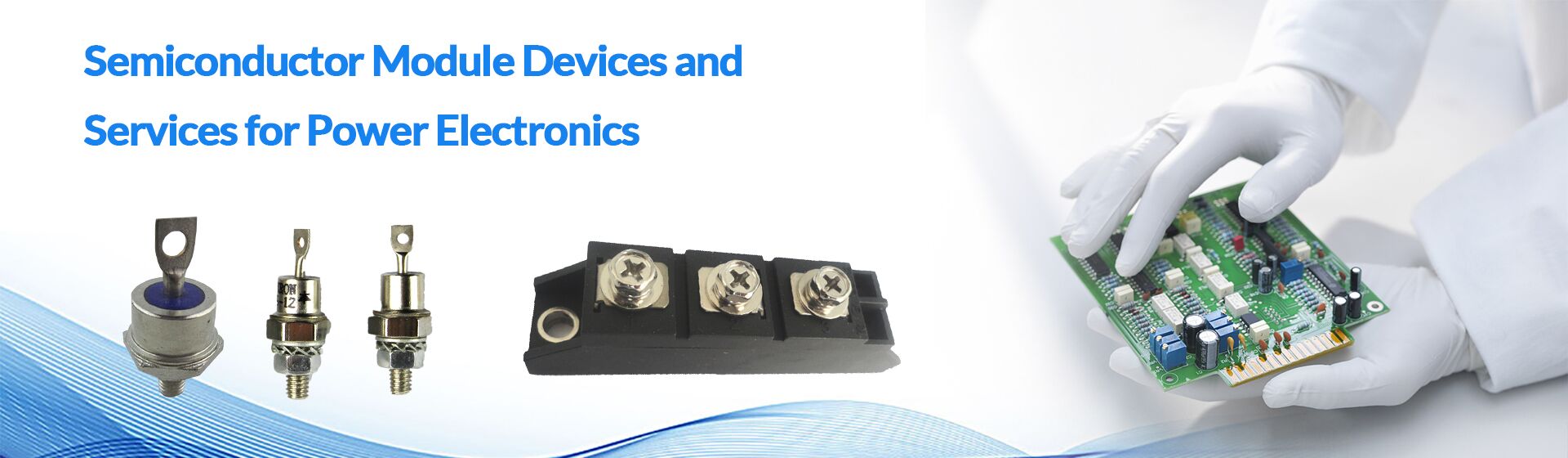
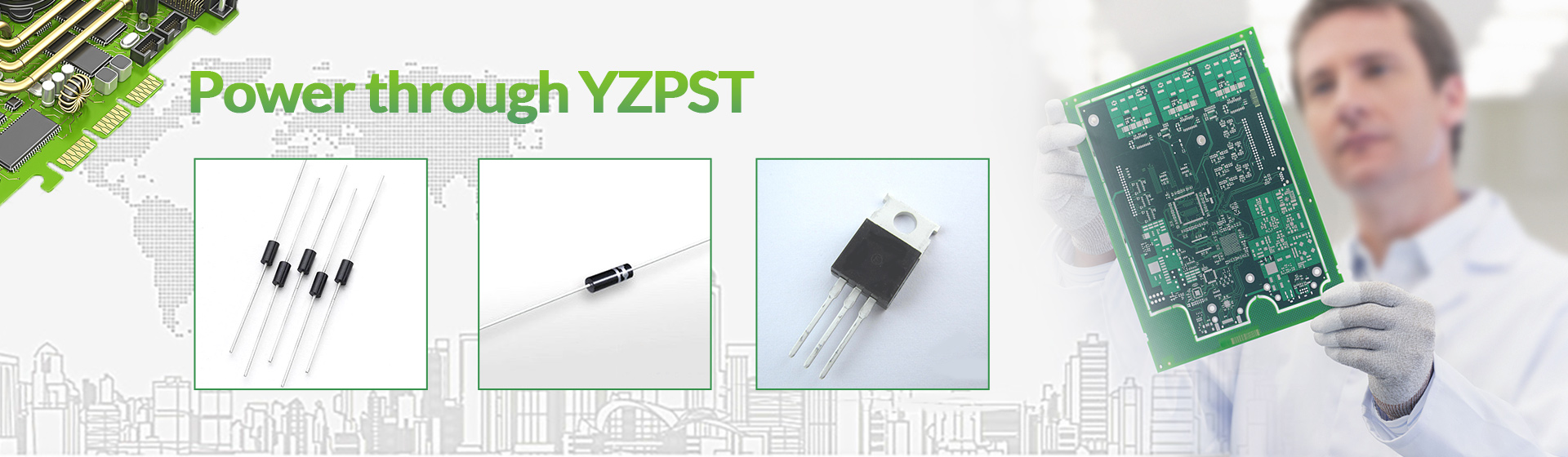
- YZPST Power semiconductor devices briefYZPST Power semiconductor devices brief Yangzhou Positioning Tech. Co., Ltd (YZPST) has her joint-venture factory which is specialized in kinds of power semiconductor devices. Such as thyristors (Phase Control Thyristors/Inverter thyristors with Stud & Capsule package), triacs, REVERSE CONDUCTING THYRISTORS(RCT), Asymmetric thyristors , series diodes(Standard and fast Recovery Diodes- with Stud & Capsule package), welding diodes ,bridge rectifier diodes, kinds of thyristor-thyristor modules, thyristor-diode modules, single diode and thyristor modules ,FRED Modules, solid state relays etc. with 20kpcs per month capacity. The company has the advanced professional production line: the high purification of workshop cleanliness up to 1000 and local up to 100 .in this line, there are many high precision diffusion furnaces, electron beam coating machines, full automatic cleaning equipments, synthesis test equipment and kind of aging inspection equipments etc. Our chief engineer comes from the famous company and has been devoted mind on kinds of power semiconductors for more than 26years . More than 30 engineers--- strong technology team to be sure that new products are continue to be developped and all products are controlled well in high class quality level .Some products have been made as per the global famous company`s spec. and exported all over the world. Our power devices are widely used for industries, public utilities and military projects. Such as transportation, marine/rail propulsion systems, frequency converter,wind power converters, electrochemical power supplies, soft starters, motor control, lighting control, power factor compensation, electric vehicles, UPS, Inverter, DC chopper drives, Pulse Power applications, High frequency, intermediate frequency welding machine, Locomotive traction, induction heating and furnaces, Steel melt shop and foundry industry, electrochemistry and military electronics.
2018 12/28
SEE MORE
Email to this supplier